High-Power Electronics
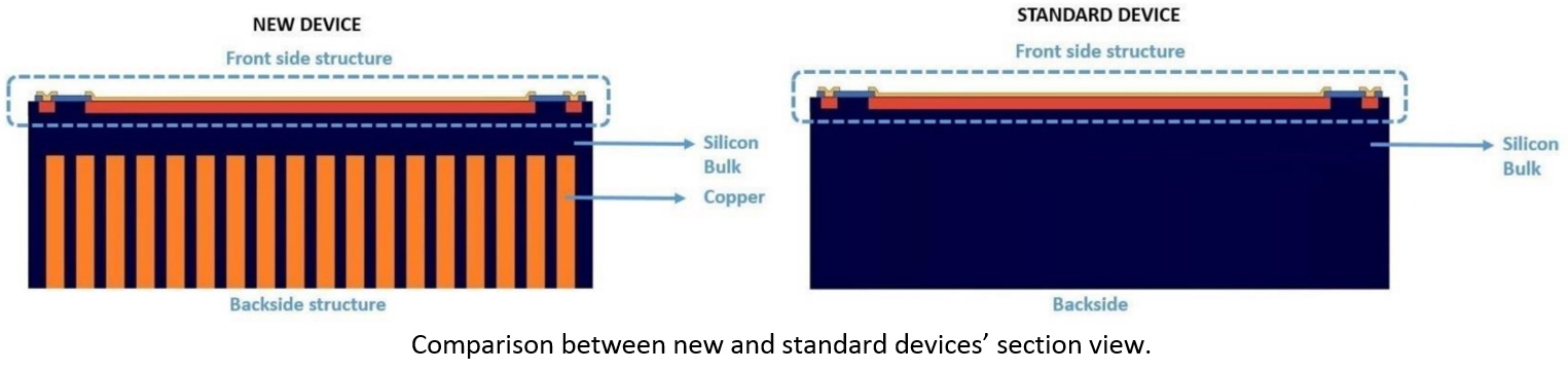
Current research activity aims to integrate copper structures in silicon thin wafers to promote thermal conductivity for high current Schottky diodes.
Thermal dissipation is an important issue in semiconductor manufacturing because the operation of a semiconductor device is sensitive to temperature. When the junction temperature exceeds its functional limit, semiconductor performance, life, and reliability can be significantly reduced. The active region of a semiconductor device is limited to the surface of the silicon wafer, thus there is a large amount of unused material. This silicon bulk material acts only as a mechanical support during manufacturing steps and limits heat dissipation during the device operation.
In electronics, the thermal resistance is a simplified parameter characterizing the devices thermal performances and it depends strongly on the wafer thickness. As mentioned before, the substrate region has no major electrical function and the thermal resistance of nearly all power chips can be significantly improved by thinning the wafer. The lower the thermal resistance, the better the thermal dissipation, thus the better the devices performance. In order to improve the thermal resistance, the thinning of the whole wafer at the back end, i.e., after the complete device processing on the front side, is strongly required. The final thickness depends on the designed package, which is determined on its own on the final customer application.
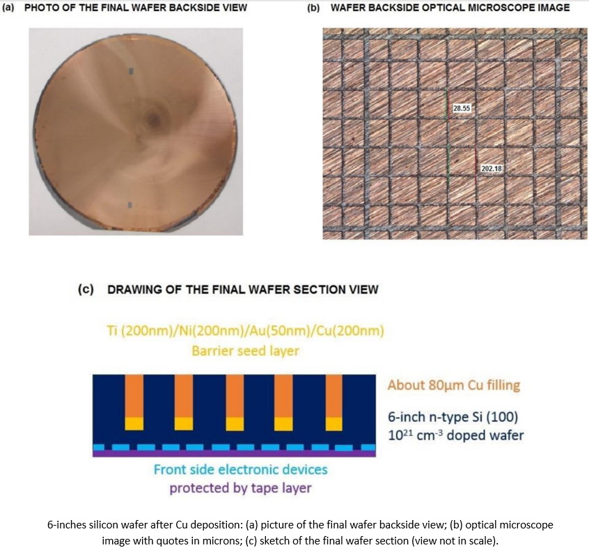
The main objective of this project is to reduce the thermal resistance of the bulk silicon without reducing the wafer thickness but by exploiting the excess material as a heat sink. The idea is to replace a large amount of bulk silicon, selectively removed by a localized wafer thinning, with a conductive material like copper.
The first goal is to develop a suitable process flow optimizing the parameters of each step and making it repeatable. The new process flow thermal and electrical performances are hence compared with those of standard devices without a modified backside. This new process flow offers the advantage of maintaining the wafer “self-support” and allows working with already existing technologies saving on both dedicated thinning and handling technologies.
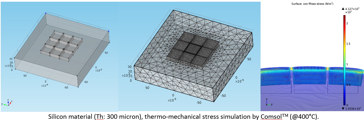
Such activity, developed in collaboration and for Vishay Semiconductor, is supported by laboratory competences in FEM simulations and clean room services to fabricate discrete electronics devices.
Contact information
Luciano Scaltrito
Tel. +39 011 090 7337
luciano.scaltrito@polito.it
Sergio Ferrero
Tel. +39 011 090 7337
sergio.ferrero@polito.it
Publications
- "Defect characterization of 4H-SiC wafers for power electronic device applications", Ferrero, S., Porro, S., Giorgis, F., Pirri, C.F., Mandracci, P., Ricciardi, C., Scaltrito, L., Sgorlon, C., Richieri, G., Merlin, L., (2002) Journal of Physics Condensed Matter, 14 (48), pp. 13397-13402
- "Low temperature growth of SiO2 on SiC by plasma enhanced chemical vapor deposition for power device applications", Mandracci, P., Ferrero, S., Ricciardi, C., Scaltrito, L., Richieri, G., Sgorlon, C., (2003) Thin Solid Films, 427 (1-2), pp. 142-146
- "Surface analysis and defect characterization of 4H-SiC wafers for power electronic device applications", L. Scaltrito, G. Fanchini, M.Cocuzza, F. Giorgis, C.F. Pirri, P. Mandracci, C. Ricciardi, S. Ferrero, C. Sgorlon, G. Richieri, L. Merlin, Diamond and related materials 12 (2003) 1224-1226
- "Structural and electrical characterization of epitaxial 4H-SiC layers for power electronic device applications", L. Scaltrito, S. Porro, M. Cocuzza, F. Giorgis, C.F. Pirri, P. Mandracci, C. Ricciardi, S. Ferrero, C. Sgorlon, G. Richieri, L. Merlin, A. Castaldini, A. Cavallini, L. Polenta, Materials Science and Engineering B102 (2003) 298-303
- "Correlation between defects and electrical properties of 4H-SiC based Schottky diodes", L. Scaltrito, S. Porro, M. Cocuzza, F. Giorgis, C.F. Pirri, P. Mandracci, C. Ricciardi, S. Ferrero, C. Sgorlon, G. Richieri, L. Merlin, A. Castaldini, A. Cavallini, Materials Science Forums 433-436 (2003) 455-458
- "Plasma-assisted SiC oxidation for power device fabrication", Mandracci, P., Ferrero, S., Porro, S., Ricciardi, C., Richieri, G., Scaltrito, L., (2004) Applied Surface Science, 238 (1-4 SPEC. ISS.), pp. 336-340
- "Defect influence on the electrical properties of 4H-SiC Schottky diodes", Scaltrito, L., Celasco, E., Porro, S., Ferrero, S., Giorgis, F., Pirri, C.F., Perrone, D., Meotto, U., Mandracci, P., Richieri, G., Merlin, L., Cavallini, A., Castaldini, A., Rossi, M., (2004) Materials Science Forum, 457-460 (II), pp. 1081-1084
- "Growth, morphological and structural characterization of silicon carbide epilayers for power electronic devices applications", Pirri, C.F., Porro, S., Ferrero, S., Celasco, E., Guastella, S., Scaltrito, L., Yakimova, R., Syväjärvi, M., Ciechonski, R.R., De Angelis, S., Crippa, D., (2005) Crystal Research and Technology, 40 (10-11), pp. 964-966
- "Phase formation at rapid thermal annealing of nickel contacts on C-face n-type 4H-SiC", Ferrero, S., Albonico, A., Meotto, U.M., Rombolà, G., Porro, S., Giorgis, F., Perrone, D., Scaltrito, L., Bontempi, E., Depero, L.E., Richieri, G., Merlin, L., (2005) Materials Science Forum, 483-485, pp. 733-736
- "Design, fabrication, and characterization of 1.5 mΩcm2, 800 V 4H-SiC n-type Schottky barrier diodes", Furno, M., Bonani, F., Ghione, G., Ferrero, S., Porro, S., Mandracci, P., Scaltrito, L., Perrone, D., Richieri, G., Merlin, L., (2005) Materials Science Forum, 483-485, pp. 941-944
- "Intrinsic 4H-SiC parameters study by temperature behaviour analysis of Schottky diodes", Pirri, C.F., Ferrero, S., Scaltrito, L., Perrone, D., Guastella, S., Furno, M., Richieri, G., Merlin, L., (2006) Microelectronic Engineering, 83 (1 SPEC. ISS.), pp. 86-88
- "Effect of defects on electrical properties of 4H-SiC Schottky diodes", Ben Karoui, M., Gharbi, R., Alzaied, N., Fathallah, M., Tresso, E., Scaltrito, L., Ferrero, S., (2008) Materials Science and Engineering C, 28 (5-6), pp. 799-804
- "Influence of inhomogeneous contact in electrical properties of 4H-SiC based Schottky diode", Ben Karoui, M., Gharbi, R., Alzaied, N., Fathallah, M., Tresso, E., Scaltrito, L., Ferrero, S., (2008) Solid-State Electronics, 52 (8), pp. 1232-1236
- "Study of the electrical characteristics of the CNT/SiC interface", Castellino, M., Bianco, S., Perrone, D., Musso, S., Giorcelli, M., Maccioni, G., Ferrero, S., Scaltrito, L., Tagliaferro, A., (2009) Materials Science Forum, 615 617, pp. 231-234
- "4H-SiC Schottky barrier diodes using Mo-, Ti- and Ni-based contacts", Perrone, D., Naretto, M., Ferrero, S., Scaltrito, L., Pirri, C.F., (2009) Materials Science Forum, 615 617, pp. 647-650
- "Barrier inhomogeneities of Mo Schottky barrier diodes on 4H-SiC", Naretto, M., Perrone, D., Ferrero, S., Scaltrito, L., (2010) Materials Science Forum, 645-648, pp. 227-230
- “Piezoelectrically actuated MEMS microswitches for high current applications”, D. Balma, A. Lamberti, S. L. Marasso, D. Perrone, M. Quaglio, G. Canavese, S. Bianco, M. Cocuzza, Microelectronic Engineering, Vol. 88(8), August 2011, Pages 2208-2210, doi: 10.1016/j.mee.2011.02.097
- "Schottky contacts to n-type 4H-SiC fabricated with Ti-, Mo-, Ni- and Al-based metallizations", Perrone, D., Ferrero, S., Scaltrito, L., Naretto, M., Celasco, E., Pirri, C.F., (2011) Materials Science Forum, 679-680, pp. 453-456
- "Barrier inhomogeneities of a medium size Mo/4H-SiC Schottky diode", Zaman, M.Y., Perrone, D., Ferrero, S., Scaltrito, L., Naretto, M., (2012) Materials Science Forum, 711, pp. 188-192
- "Fabrication of Ni/Ti/Al Schottky contact to n-type 4H-SiC under various annealing conditions", Zaman, M.Y., Ferrero, S., Perrone, D., Scaltrito, L., Shahzad, N., Pugliese, D., (2013) Journal of Physics: Conference Series, 439 (1), art. no. 012027
- "Series resistance study of Schottky diodes developed on 4H-SiC wafers using a contact of titanium or molybdenum", Shili, K., Ben Karoui, M., Gharbi, R., Abdelkrim, M., Fathallah, M., Ferrero, S., (2013) Microelectronic Engineering, 106, pp. 43-47
- "Structural and electrical characterization of the 4H-SiC based junction field effect transistor (JFET)", Shili, K., Ben Karoui, M., Gharbi, R., Ferrero, S., 2013 International Conference on Electrical Engineering and Software Applications, ICEESA 2013, art. no. 6578475
- "Convective heat transfer enhancement for electronic device applications using patterned MWCNTs structures", M. I. Shahzad, M. Giorcelli, L. Ventola, D. Perrone, N. Shahzad, E. Chiavazzo, P. Asinari, M. Cocuzza, A. Tagliaferro, Heat Transfer Engineering, August 2015, DOI: 10.1080/01457632.2015.1080570
- "Barrier height evolution in a non-uniform interface of Ti or Mo Schottky diodes based on 4H-SiC", Gharbi, R., Shili, K., Ben Karoui, M., Fathallah, M., Ferrero, S., (2016) International Journal of Electronics Letters, 4 (3), pp. 367-375
- "Back plate electroplating for high aspect ratio processes", S.L. Marasso, S. Benetto, I. Para, C. Ottone, D. Mombello, D. Perrone, S. Ferrero, L. Scaltrito, D. Pugliese, M. Cocuzza, C.F. Pirri, Microelectronics International, 2017, Vol. 34(2), pp. 69-74, doi:10.1108/MI-03-2016-0024
- "Wafer level integration of 3D heat sinks in power ICs", I. Para, S. L. Marasso, D. Perrone, M. G. Gentile, C. Sanfilippo, G. Richieri, L. Merlin, D. Pugliese, M. Cocuzza, S. Ferrero, L. Scaltrito and C. F. Pirri, IEEE Transactions on Electron Devices, 2017, 64 (10), 4226-4232, doi:10.1109/TED.2017.2732733
Partners & Collaborations
Vishay International S.p.A.
Novasis Innovazione s.r.l.