CMOS sensor characterization
Characterization of Monolithic Active Pixel Sensors produced following CMOS 180 nm process for the upgrade of the ALICE experiment
Introduction. The ALICE experiment (see ALICE info page) will be upgraded in 2019-2020, during Long Shutdown
2 (LS2) of the CERN Large Hadron Collider (LHC), enhancing its physics capabilities concerning mainly high precision measurements of rare probes at low transverse momenta.
The innermost detector of the experiment is the so-called Inner Tracking System (ITS). At present it is composed by six layers of silicon detectors.
The current ITS will be replaced by seven concentric layers 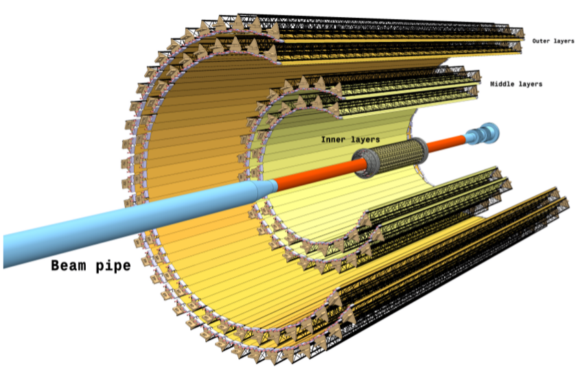 of Monolithic Active Pixel Sensors (MAPS) with total active surface of 10 m2, thus making ALICE the first
LHC experiment implementing MAPS detector technology on a large scale.
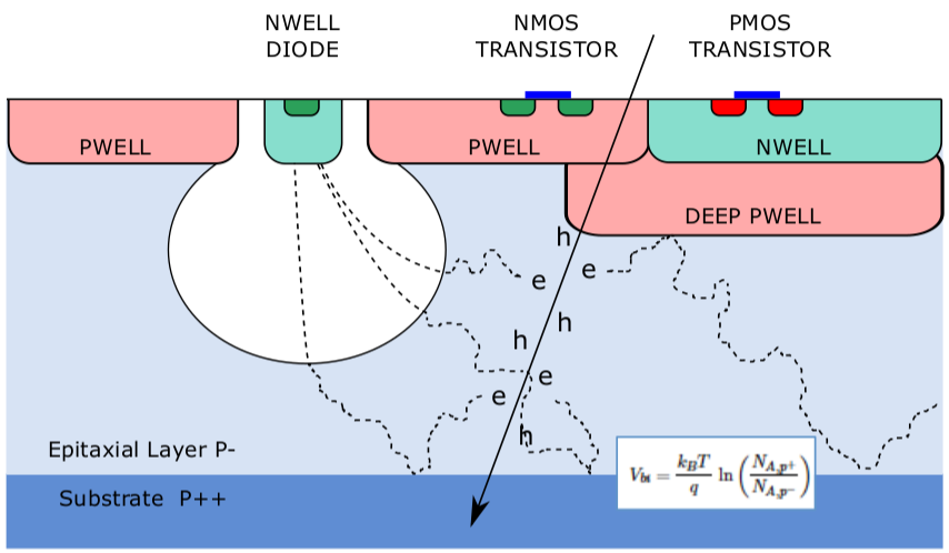
The ALPIDE (ALice PIxel DEtector) chip, based on TowerJazz 180 nm CMOS Imaging Process, is being developed for this purpose. A particular process feature, the deep p-well, is exploited so the full
CMOS logic can be implemented over the active sensor area without impinging on the deposited charge collection. ALPIDE is implemented on silicon wafers with a high resistivity
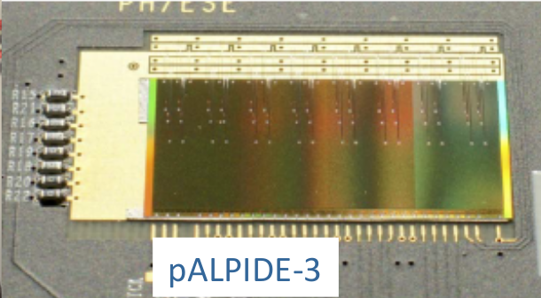
epitaxial layer. A single chip measures 15 mm by 30 mm and contains half a million pixels distributed in 512 rows and 1024 columns. In-pixel circuitry features amplification,
shaping, discrimination and multi-event buffering. The readout is hit driven i.e. only addresses of hit pixels are sent to the periphery.
The upgrade of the ITS presents two different sets of requirements for sensors of the inner and of the outer layers due to the significantly different track density, radiation level
and active detector surface. The ALPIDE chip fulfils the stringent requirements in both cases. The detection efficiency is higher than 99%, fake hit probability is orders of
magnitude lower than the required 10- 5 and spatial resolution within required 5 μm. 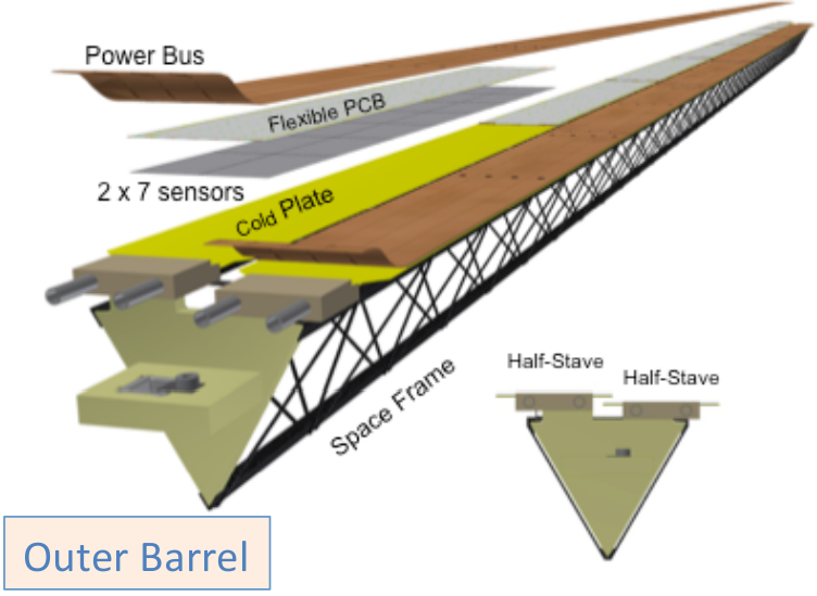 This performance is maintained even after an irradiation up to several Mrad and
few 1013 1 MeV neq/cm2, which is above what is expected during the detector lifetime. Readout rate of 100 kHz is provided and the power density
of ALPIDE is less than 40 mW/cm2.
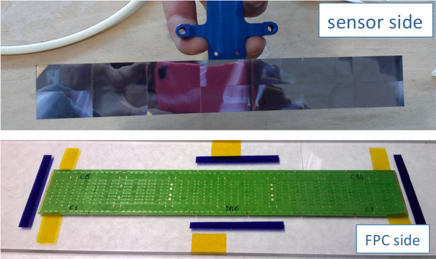
Considering the four outermost layers, the ALIPIDE chip will be arranged in Modules, structures containing 14 chips arranged in two independent rows of 7 chips. A Master-Slave
communication (1 master and 6 slaves per row) is envisaged. The master receives the clock and control signals from the outside and sends out the data of itself and of the six slaves.
All signals are differential (LVDS) and run on a flex circuit (FPC) wire-bonded to the 14 chips. Also the analog and digital voltages are provided by means of the FPC, but
with the help of a Power Bus (PB) preventing high voltage drops along the line.
Each module is about 21 cm by 3 cm and, the two outermost layers will have seven modules composing the so-called half-stave for a total length of 1.5 m.
Thesis objective. This is an experimental thesis in physics/electronics. Entering into an international collaborarion (ALICE collaboration), the thesis consists in the
characterization, from an electronic point of view, of an ALICE ITS Module. In particular, during the thesis period, a subset of the following measurements can be done:
- Supply current profiles:
- measure current and voltage profile with digital injections (in collaboration with CERN);
- compare current and voltage profiles with and without clock gating (in collaboration with CERN);
- Test of control communication:
- determine digital voltage working range (in collaboration with INFN Bari);
- Signalling:
- measure output signal shape after FPC + 5 m cable varying the digital voltage and driver settings;
- Readout performance:
- determine digital voltage working range (in collaboration with INFN Bari);
- compare error rate for single chip readout vs. concurrent readout (in collaboration with INFN Bari);
- measure error rate as a function of trigger frequency and occupancy (in collaboration with INFN Bari);
- Analogue performance:
- threshold and noise occupancy scans at different back-bias and analogue voltages;
- compare threshold and noise occupancy for single chip and concurrent readout;
- try to equalize chip thresholds and lower thresholds, compare fake hit rate to single chips;
- noise occupancy measurement at low threshold vs trigger rate with simultaneous injections;
- threshold scans and noise occupancy as a function of the temperature.

To obtain more information or submit your candidature: beole@to.infn.it; michelangelo.agnello@polito.it; ivan.ravasenga@polito.it


