Laboratory of Theoretical and Experimental Superconductive Tunnelling |
| Home | Publications | Equipments | Projects | People | Join us | Links |
Fundamental study of unconventional superconductors | Experimental technique The so-called field effect consists in the modulation of the conduction properties of a material (that forms the channel) by means of a transverse dc electric field. The field effect is widely used in nowaday's electronics (field-effect transistors, FET). Conventional field-effect devices are made by using a solid dielectric to separate the channel from the gate electrode. In these devices, the breakdown field and the thickness of the dielectric limit the maximum achievable intensity of the electric field. Polymeric electrolyte solutions (PES) or ionic liquids (IL) allow considerable increase in the field intensity, thanks to the formation of an electric double layer (EDL) at the interface with the channel. Here, charged ions accumulate creating a "capacitor" whose inter-plate spacing is of the order of the molecule size (i.e. a few nanometers). By using a novel PES we were able to obtain unprecedented high fields, and thus surface densities of charge, in noble metals (Au, Cu, Ag). This "charge" doping gave rise to an increase in the conductance of these metals (10% in Au at low temperature). The same approach is used to test the effects of large charge injections on the conduction properties of various materials, including:
| 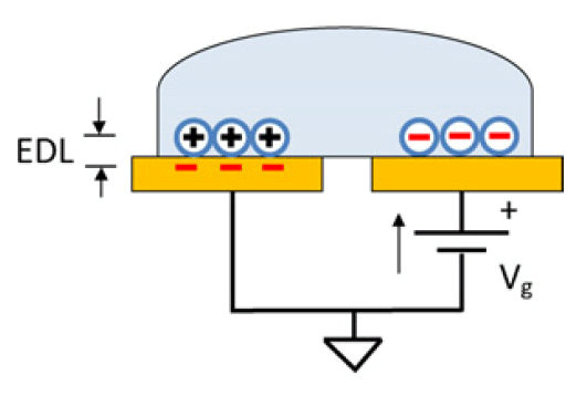 Working principle of an EDL FET. The active channel is on the left, the gate electrode on the right. 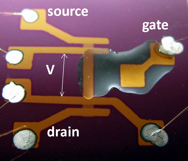 Photo of an EDL FET made of a Au channel deposited on a silicon-oxide substrate. The drop of PES connects the channel to the gate electrode. 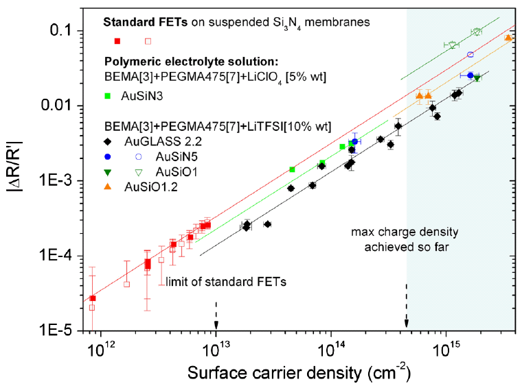 Relative resistance variation of gold thin films (at room temperature) as a function of the surface charge density induced by the electric field |
| LaTEST - Department of Applied Science and Technology, Politecnico di Torino corso Duca degli Abruzzi 24, 10129 Torino (TO) - Italy  |