MEMS & Microsensors
The Laboratory boasts a long-term experience in the design and fabrication of MEMS and microsensors and is equipped with a broad portfolio of technologies for the implementation of the main processes at the microscale for the fabrication of MEMS and microsystems:
- technologies for the growth of thin films both conductive and dielectric (thermal and e-gun evaporation of metals, Plasma Enhanced Chemical Vapor Deposition (PECVD), Low Pressure Chemical Vapor Deposition (LPCVD), magnetron sputtering, silicon oxidation, Electroplating, Rapid Thermal Annealing (RTA)) or active materials (magnetic, piezoelectric by sol-gel deposition or sputtering, …);
- lithographic technologies for devices patterning (optical lithography with front & backside alignment, LIGA-like processes using SU-8, laser lithography (Direct Laser Writing) for the direct exposure of photoresist or the manufacture of masks);
- technologies for wet etching, dry etching (plasma etcher, Reactive Ion Etcher, Deep Reactive Ion Etcher (DRIE) with implementation of both Bosch ® and cryogenic techniques) and physical etching (micro powder blasting);
- technologies for polymers (thermoplastics, elastomers, photocurable polymers and composites) microscale processing (Hot Embossing, Micro Injection Moulding, Casting in Situ);
- technologies for Rapid Prototyping & Additive Manufacturing (3D Polymer Ink-Jet Printing, Micro Stereo Lithography, Micro Electro Discharge Machining, Direct Polymer Laser Sintering, CNC Milling) on both polymers and metals;
- technologies for the implementation of Laser Micromachining processes (marking, drilling, cutting, engraving, ...) on different materials;
- technologies for the modification and functionalization of active surfaces (wet functionalization, Low and Atmospheric Plasma Polymerization).
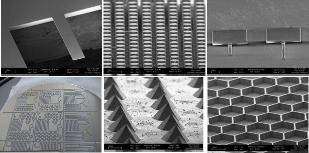
Such technologies can be used for the development of process flows for the manufacture of various types of suspended microstructures (microcantilevers, micromembranes, microbridges, ...) and microstructures characterised by high aspect ratio both above the surface of the substrate or deeply etched in the same, for the fabrication of MEMS and microsensors by Bulk Micromachining, Surface Micromachining and LIGA-like Micromachining.

Such microstructures can then be suitably transformed into highly specialized microsensors, or in arrays of the same, by integration of active materials or functionalization of the surfaces to provide them with a specific function for sensing or target capture capability.
So far we developed several MEMS devices and microsensors prototypes for different application fields, among which we mention:
- gravimetric microsensors (microcantilevers), also in the form of an array, for chemical and biological sensing and for pressure (vacuum) measuring;
- the same microstructures have also been employed as actuators (microrelay for industrial automation) and could be used as transducers for Energy Harvesting;
- hazardous and combustible gas microsensors based on micro hot-plate technology and integration of a proper nanostructured active material;
- microfluidic devices (Lab-On-a-Chip) fabricated either by the classical silicon-glass pair or with polymeric materials, also integrating proprietary and third-party sensing elements;
- sensors and sensor arrays based on electrical transduction (Multi Electrode Arrays, Organic Electrochemical Transistors (OECTs), EGOFETs, …) both on silicon and flexible (kapton) substrates;
- molecular sieves (He) prepared by glass Bulk Micromachining for vacuum industrial applications.


More generally, the Laboratory is able to implement solutions for the development of processes for the manufacture of MEMS devices prototypes, microsensors and microactuators, eventually integrated with advanced or innovative functional materials, with a high degree of specialization and customization with respect to the requirements.
Contact information
Matteo Cocuzza
Tel. +39 011 090 7392
matteo.cocuzza@infm.polito.it
Simone Marasso
Tel. +39 011 911 4899
simone.marasso@polito.it


