Laser Micromachining
Laser Micromachining
Since the year 2000 the Chilab was involved in the exploitation of lasers potential in micromachining. At the end of 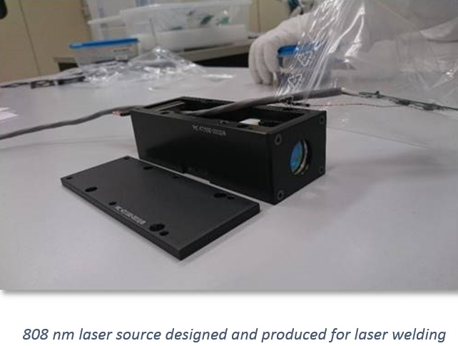 the year 2002 the lab began to design the first Diode Pumped Solis State Laser for High Peak Power generation, in collaboration with Zaniboni Laser s.r.l. to develop laser marker machines. Up to now several different laser sources have been designed and tested. Moreover, in 2006 the lab decided to found a new Spin-Off dedicated to the design and fabrication of lasers for materials processing such as marking, micro-drilling, micro-cutting and micro-welding. Microla Optoelectronics s.r.l. (http://www.micro-la.com) skills range from the fabrication of laser sources to the optical and thermo-dynamical design of laser systems and the feasibility study of processes based on these sources.
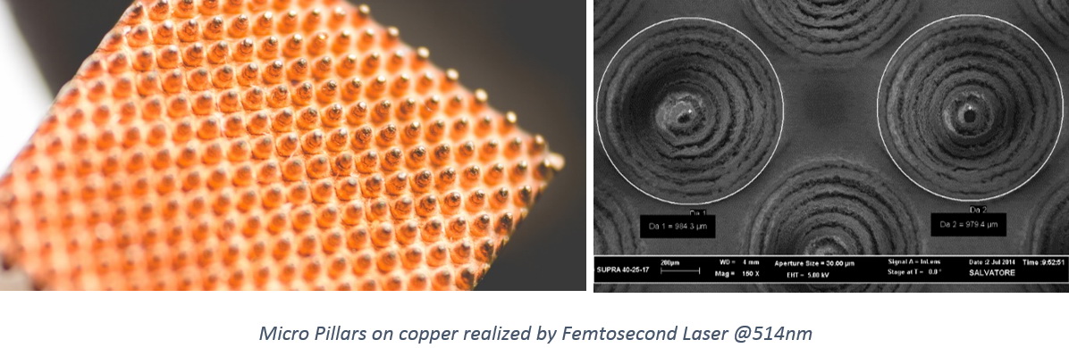
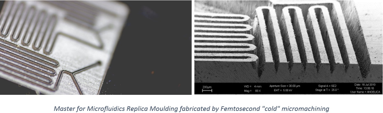
Laser micromachining techniques such as metal micromachining (micro drilling and micro milling), ultra-short pulses and femtosecond pulses are used in micro fabrication. Lasers allows the manufacturing of micro sized MEMS parts, precision cutting of glass, small-hole drilling for gas leakage applications, cutting of PCB and various polymides. While nanosecond sources are used for generic marking, cutting and drilling applications, femtosecond lasers are used for "cold" ablation, notably the drilling and cutting of high-precision holes (such as in the production of medical stents) free from thermal damage. The ultrafast lasers essentially vaporize matter without generating heat, creating new ways to machine materials. They are particularly suitable for the machining of very small, very precise patterns in tough materials. The ability of femtosecond lasers to efficiently fabricate complex structures and devices for a wide variety of applications has been extensively studied during the last decade. State-of-the-art laser processing techniques with ultrashort light pulses can be used to structure materials with a sub-micrometer resolution. Several applications have been faced ranging from microfluidic devices, heat transfer, chalcography and master for moulding.
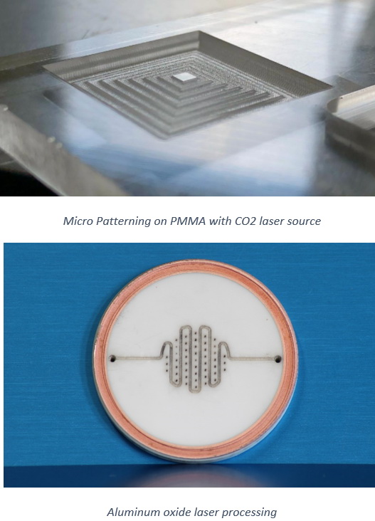 The Laser Direct Patterning can performed on several materials such as: FR4, Vetronite, Bakelite, IMS and standard packages for semiconductors. Lasers, such as Nd:YAG lasers and their harmonics are used for a variety of precision machining operations and are particularly well-suited for micromachining of polymer materials or the marking of materials such as metals and diamonds. Infra-red low power lasers such as CO2 are used for engraving. The common poly (methyl methacrylate) (PMMA) absorbs IR light in the 2.8–25 µm wavelength band, so CO2 lasers have been used for fabricating microfluidic devices with channel widths of a few hundreds micrometers, as well as to produce micropatterning on PMMA surface. Similarly, through green nanosecond sources holes and channels have been precisely realized on Aluminium oxide for a device for vacuum applications.
Contact information
Luciano Scaltrito
Tel. +39 011 090 7337
luciano.scaltrito@polito.it
Sergio Ferrero
Tel. +39 011 090 7337
sergio.ferrero@polito.it
Laser-induced graphenization
Laser-induced graphene (LIG) obtained by laser writing of polymeric substrates has been recently reported as an incredibly promising material for flexible electronics. It consists of a three-dimensional network of few layer graphene obtained by a laser writing process of the polymeric surface (Figure 3).

Photograph and FESEM images at different magnifications of the obtained LIG on polyimide foil
These conductive paths obtained on flexible substrate can be exploited for the fabrication of supercapacitors, batteries, photoelectrochemical solar cells, electrochemical sensors and many other devices that can take advantage from a porous high-surface-area graphene-based network on polymeric substrate.
Contact Information
Andrea Lamberti
Tel. +39 011 090 7394
andrea.lamberti@polito.it