Microfluidics
The Laboratory owns a robust experience and a large set of technologies for the implementation of the main processes for the fabrication of microfluidic devices and Lab-On-a-Chip for different applications.
With regard to microfluidics, we can cover the entire development flow: from the design of a customised microfluidic solution and FEM simulation of the most critical components, passing through the implementation of several front-end and back-end processes on different materials for the fabrication of prototypes, up to the microfluidic characterization and testing. Whenever possible or useful we can also support our partners for the functional test and eventually for the development of a fully automatic or semi-automatic platform.
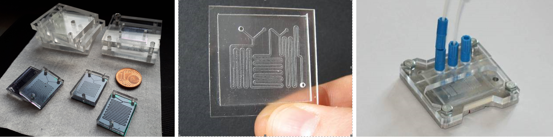
Apart from the standard silicon-glass pair, we can machine and deal with a large set of different materials, according to the specific application requirements: thermoplastics (PMMA, PC, COC, COP, …), elastomers (PDMS), elastomer-based composites (i.e. carbon-based materials in a PDMS matrix), photosensitive resins (SU-8) and photocurable polymers (i.e. PFPEs), these latter also with a 3D printing approach.
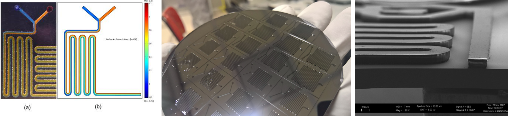
Concerning the silicon-glass pair, we can etch microchannels and microfluidic components on both of them by wet etching (KOH and BOE respectively), dry etching (RIE and DRIE through Bosch® and Cryogenic approaches) or micro powder blasting. The two parts are then assembled by anodic bonding.
For most of the polymeric materials the manufacturing approach is that based on polymeric replication. We can fabricate a master with the proper features (i.e. in terms of layout, resolution, number of devices, …) through standard micromachining techniques and then replicate the same onto thermoplastics (by hot embossing or injection moulding) or elastomers (by casting in-situ). We can also support the partner requiring a small volume production capability, thanks to a micro injection moulding system suitable to allow for a relatively low cost fabrication lot.
Photosensitive or photocurable polymers are transformed into microfluidics by direct UV exposure with a standard mask aligner and through a mask or eventually by direct laser writing for advanced requirements in terms of resolution. Microstereolitography and 3D Printing are further options to build relatively complex multi-layered microfluidic devices or for back-end needs to support microfluidic components and associated assembly by a rapid prototyping approach.
During the last ten years we have developed research devices and prototypes for commercial purposes for extremely diversified application fields: genomic and proteomic analysis and diagnostics, cell analysis, water monitoring, chemical reactors and energy conversion oriented micro-devices (fuel cells, Dye Sensitized Solar Cells).
A significant effort, usually for mid to long-term chemical and biological applications, is currently spent for the integration of microfluidic devices with advanced sensing tools, for instance to improve the performances of sensors and diagnostic platforms, mainly but not only in terms of sensitivity, which is absolutely the main issue along the road towards a real early diagnostics approach. Concerning this last issue, we have matured a significant experience for instance in the fabrication and microfluidic integration of gravimetric sensors (microcantilevers), photonic devices and enhanced optical detection tools (plasmons, Surface Electromagnetic Waves, …) and electronic devices (i.e. Organic Electro Chemical Transistors).
In conclusion, the Laboratory holds both the skills and the facilities for the implementation of processes for the manufacture of microfluidic devices and prototypes, according to different and specific application requirements, and eventually integrated with proprietary or third-party functional materials and sensors.
Contact information
Matteo Cocuzza
Tel. +39 011 090 7392
matteo.cocuzza@infm.polito.it
Simone Marasso
Tel. +39 011 911 4899
simone.marasso@polito.it