Atomic Layer Deposition (ALD)
Atomic Layer Deposition (Beneq TFS200)
 ALD allows depositing thin films with atomic layer control in a simple and reproducible process, with low impurity contamination, for a variety of applications, with possibility of deposition on very high aspect/ratio structures that need to be coated conformally. No other thin film technique can approach the conformality achieved by ALD on high aspect ratio structures.
ALD is able to meet the needs for atomic layer control and conformal deposition using sequential, self-limiting surface reactions. The advantages of ALD are precise thickness control at the Ångstrom or monolayer level. The self-limiting aspect of ALD leads to excellent step coverage and conformal deposition on high aspect ratio structures. ALD films remain extremely smooth and conformal to the original substrate because the reactions are driven to completion during every reaction cycle.
Low temperature ALD enables ALD on thermally sensitive materials such as organic polymers. ALD on polymers may be useful to functionalize the polymer surface, to create unique inorganic/organic polymer composites, and to deposit gas diffusion barriers on polymers.
ALD process is based on the principle of sequential pulsing of the vapours of precursor chemicals, where nearly one atomic layer is formed for each pulse. Between the reactant pulses, excess reactants and reaction by-products are purged out or evacuated.
ALD growth of oxide thin films is promising due to their broad range of electrical properties extending from insulating, semiconducting, metallic to superconducting. ALD is used in our lab mainly for the deposition of oxide thin layers for the fabrication of memristor-type switching devices, based on alumina (Al2O3), titania (TiO2) or tantalum oxide (TaOx, Ta2O5). For instance, ALD favours the growth of pure, crystalline titania thin films. TiO2 films grown at low temperatures are generally flat and amorphous and are grown at different substrates such as polymer templates, polymer fibers, and so on.

FESEM image of the cross section of a thick (~450 nm) TiO2 anatase polycrystalline layer deposited by ALD on a silicon wafer, showing the presence of large-size columnar growth of TiO2 crystals
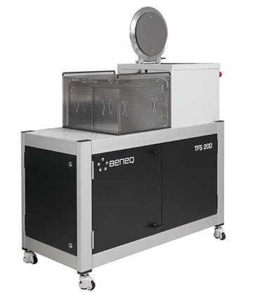
The Beneq TFS200 installed in our Lab is an ALD tool for thin film processing. It is based on a hot wall, flow-through type reaction chamber. The reaction chamber is located inside a water cooled cold wall vacuum chamber. The system is equipped with a single wafer reaction chamber. Substrates can be silicon wafers (up to 8”) or other planar substrates. The uniformity of deposition is guaranteed also on high aspect-ratio structures (up to 50).
The TFS200 ALD system is designed especially for research purposes, which set high demands on flexibility and usability. These demands are met by a highly modular structure. The precursor source modules, reaction chambers and control system use proven technical solutions. TFS 200 has compact footprint and is equipped with a compact, easy to use reaction chamber.
The hot wall reaction chamber is located inside the cold wall vacuum chamber. The vacuum chamber is located on the top of the system and it is equipped with a loading lid. The reaction chamber lies right under this lid. The heating system is internal and directly connected to the reaction chamber bottom plate. The control system has a Laptop PC interface running the Beneq control software. The hardware is based on Siemens S7 PLC, a highly reliable industrial logic.
The system is currently equipped with three room-temperature liquid sources, one HS300 hot source with two interchangeable precursor containers (for liquid and solid precursor materials which need heating to reach sufficient vapor pressure, up to 300°C), and an ozone (O3) gas line. The liquid sources are located in an aluminum block, which is temperature stabilized with a controlled water circulation. The hot source is located right beside the vacuum chamber. This layout allows robust, heated, short and wide hot source feeding lines with high conductance and low pressure drop to maximize the source output. This setup is currently used for deposition of Al2O3, TiO2, ZnO, and Al-doped ZnO (AZO) (liquid source) and Ta2O5 (hot source) thin layers.
In addition, the full ozone line (including ozone generator) allows the deposition of other types of materials, such as Fe oxides (hematite, magnetite).