Experimental facilities
- Systems for Thin-film Growth and Surface Treatments
- LPCVD
- Furnace System
- Thermal & E-Gun Evaporation
- Sputtering
- PZT sol-gel
- Rapid Thermal Annealing (RTA)
- Electroplating
- Low Pressure Plasma Polymerization System
- ECR/RF PECVD deposition system
- RF Magnetron sputtering (monotarget)
- Atmospheric Pressure Plasma System
- Single-layer Graphene growth
- Atomic Layer Deposition (ALD)
- ICPCVD
- Parylene Deposition
- Cleanrooms
- Rapid Prototyping & Additive Manufacturing
- Lithographic Tools
- Etching Facilities
- Polymeric Machining
- Chemical & Bio-chemical Labs
- Characterizations
- Optical Microscopy
- Profilometry
- Microfluidic test
- Piezoelectric Characterization
- Fluorescence Microscopy
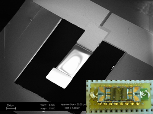
- Electron Microscopy 1
- Electron Microscopy 2
- Advanced Optical Microscopy
- Raman Spectroscopy 1
- Raman Spectroscopy 2
- FT-IR Spectroscopy
- X-ray Photoelectron Specroscopy
- Optical Contact Angle
- UV-Vis Spectroscopy
- Fluorescence Spectroscopy
- Conductive Atomic Force Microscopy
- Electrical and Electrochemical characterization
- BET
- Nanomechanical sensing
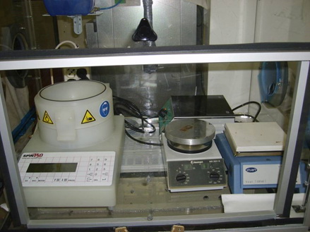
PZT sol-gel
Home-assembled glove box equipped with spinner for sol dispensing and spinning and with 3 hot plates for PZT thin films thermal processing.